
派瑞林防水
News
At Diamond MT we often get the question: “Can my xxx be parylene coated?” The number of substrate surfaces that can be coated with parylene is plenty. In the table below a number of industrial applications that using Parylene conformal coatings are listed. The examples can be extended.
Table: Examples of devices that make use of Parylene conformal coatings.
|
Printed circuit boards |
Implantable devices |
Optical lenses |
|
MEMs |
Valves |
Power Supplies |
|
LEDs |
O-rings |
Backplanes |
|
Catheters |
Tubing |
Photoelectric Cells |
|
Stents |
Silicon Wafers |
Forceps |
|
Magnets |
Keypads |
Test tubes |
|
Paper |
Stoppers |
Probes |
|
Needles |
Seals |
Fiber Optic Components |
|
Sensors |
Mandrels |
Pace-makers |
|
Ferrite Cores |
Molds |
Bobbins |
|
Metallic Blocks |
Motor Assemblies |
And many more… |
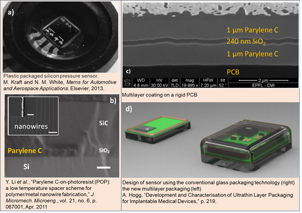
Substrate surface / Parylene interaction / Substrate surface preparation, interface cleanliness, surface energy: By Parylene CVD deposition it is possible to obtain stress-free and defect-free conformal coatings on almost all types of materials. Some examples of such coatings are shown in the Figure. (a) Sensors used in the automotive industry can be prone to high temperatures, hydrocarbons, moisture. Such environments cause the sensors Aluminum contact pads to corrode quickly. Use of parylene on these pads protect them and is commonly employed [1]. (b) Parylene is also used as a masking material in MEMS devices due to its capability to fill the crevices, in the image it fills under the undercut and act as a spacer to produce 100 nm wide nanowires (inset). In that study, it forms interfaces with a polymeric resist, Silicon, Silicon Carbide and Platinum [2]. In the figure (c and d) we see that the parylene can be applied to replace the glass packaging leading to a smaller dimension and weight in the package. Also, the parylene can be coated as a stack of layers combined with other thin layers such as SiO2 as shown in image c. The diversity in the applications and possibilities makes the Parylene a very attractive conformal coating.
However, there are a few steps to follow before starting the deposition process. To prevent delamination, pinholes, cracks, wrinkles, blisters and other types of thin film defects different types of surfaces require different surface preparations. We discuss some of the common types below as bullet points:
Example Parylene/Material systems:
PCB: The most common application area of Parylene is PCBs as a protective coating of the electronic components, bonds and the wires. It forms a protective layer against mechanical impact and diffusion of corrosive elements [11].
Silicon Wafer: Wafer bonding intermediate layers [12], as a mask for silicon chemical etching [13],
Ceramic / Glass: A-174 silane solution pretreatment can improve the adhesion of the Parylene-C thin film on flat glass substrate specimens [14].
Metals / Alloys: Parylene is widely used in coating sensor pads. (Figure (a) shows a plastic packaged silicon pressure sensor [1]) Parylene suffers from poor adhesion to itself and noble metals, such as gold and platinum. To promote their adhesion a commercially available adhesion promoter can be used and it was reported that a 100-fold increase in adhesive strength at such interfaces was achieved and the corresponding improvements in resistance to moisture driven delamination were observed[15].
Parylene – Metal – Parylene sandwich structures are produced as flexible electrodes, sensors, in general as biocompatible implants [16]–[18].
Parylene – Parylene deposition is possible but requires post-treatment to form a chemically stable interface by thermal treatment [16], [19].
Polymers: Parylene C on photoresist can be achieved by improving the adhesion of the resist and Parylene introducing a modified silanization pretreatment including heat treatment to remove hydroxyl groups from the surface of the resist. [2]
On oil: When the vapor pressure of the oil is low (<5 Pa) it is possible to deposit parylene on top[3]. Parylene coated on oil exhibits a small stress and it can be ignored [4]. Parylene-on-oil deposition (CVD) has been used for the preparation of long-term implantable pressure sensors [5], optical lenses out of oil [6]–[8] and to make isolated parylene films by separating the parylene after deposition [9], [10].
REFERENCES
[1] M. Kraft and N. M. White, Mems for Automotive and Aerospace Applications. Elsevier, 2013.
[2] Y. Li et al., “Parylene C-on-photoresist (POP): a low temperature spacer scheme for polymer/metal nanowire fabrication,” J. Micromechanics Microengineering, vol. 21, no. 6, p. 067001, Apr. 2011, doi: 10.1088/0960-1317/21/6/067001.
[3] A. Homsy et al., “Solid on liquid deposition, a review of technological solutions,”Microelectron. Eng., vol. 141, pp. 267–279, Jun. 2015, doi: 10.1016/j.mee.2015.03.068.
[4] “Tensile Film Stress of Parylene Deposited on Liquid | Langmuir.” https://pubs.acs.org/doi/10.1021/la102790w (accessed Apr. 26, 2020).
[5] A. M. Shapero, Y. Liu, and Y.-C. Tai, “Parylene-on-oil packaging for long-term implantable pressure sensors,” Biomed. Microdevices, vol. 18, no. 4, p. 66, Jul. 2016, doi: 10.1007/s10544-016-0089-4.
[6] Binh-Khiem Nguyen, Eiji Iwase, Kiyoshi Matsumoto, and Isao Shimoyama, “Electrically driven varifocal micro lens fabricated by depositing parylene directly on liquid,” in 2007 IEEE 20th International Conference on Micro Electro Mechanical Systems (MEMS), Jan. 2007, pp. 305–308, doi: 10.1109/MEMSYS.2007.4433059.
[7] T. Kan, H. Aoki, N. Binh-Khiem, K. Matsumoto, and I. Shimoyama, “Ratiometric Optical Temperature Sensor Using Two Fluorescent Dyes Dissolved in an Ionic Liquid Encapsulated by Parylene Film,” Sensors, vol. 13, no. 4, pp. 4138–4145, Apr. 2013, doi: 10.3390/s130404138.
[8] W. F. Gorham, “A New, General Synthetic Method for the Preparation of Linear Poly-p-xylylenes,” J. Polym. Sci. [A1], vol. 4, no. 12, pp. 3027–3039, 1966, doi: 10.1002/pol.1966.150041209.
[9] H. Keppner and M. Benkhaira, “Method for producing a plastic membrane device and the thus obtained device,” US20090246546A1, Oct. 01, 2009.
[10] N. Binh-Khiem, K. Matsumoto, and I. Shimoyama, “Porous Parylene and effects of liquid on Parylene films deposited on liquid,” in 2011 IEEE 24th International Conference on Micro Electro Mechanical Systems, Jan. 2011, pp. 111–114, doi: 10.1109/MEMSYS.2011.5734374.
[11] A. Hogg, “Development and Characterisation of Ultrathin Layer Packaging for Implantable Medical Devices,” p. 219.
[12] H. Noh, K. Moon, A. Cannon, P. J. Hesketh, and C. P. Wong, “Wafer bonding using microwave heating of parylene intermediate layers,” J. Micromechanics Microengineering, vol. 14, no. 4, pp. 625–631, Apr. 2004, doi: 10.1088/0960-1317/14/4/025.
[13] Hsi-wen Lo, Wen-Cheng Kuo, Yao-Joe Yang, and Yu-Chong Tai, “Recrystallized parylene as a mask for silicon chemical etching,” in 2008 3rd IEEE International Conference on Nano/Micro Engineered and Molecular Systems, Jan. 2008, pp. 881–884, doi: 10.1109/NEMS.2008.4484464.
[14] “The Adhesion Properties of Parylene-C Thin Films | Scientific.Net.” https://www.scientific.net/AMM.421.337 (accessed Apr. 26, 2020).
[15] “Characterization and Modification of Adhesion in Dry and Wet Environments in Thin-Film Parylene Systems - IEEE Journals & Magazine,” Accessed: Apr. 26, 2020. [Online]. Available: https://ieeexplore.ieee.org/abstract/document/8418313.
[16] R. P. von Metzen and T. Stieglitz, “The effects of annealing on mechanical, chemical, and physical properties and structural stability of Parylene C,” Biomed. Microdevices, vol. 15, no. 5, pp. 727–735, Oct. 2013, doi: 10.1007/s10544-013-9758-8.
[17] W. Li, D. C. Rodger, E. Meng, J. D. Weiland, M. S. Humayun, and Y.-C. Tai, “Flexible Parylene Packaged Intraocular Coil for Retinal Prostheses,” in 2006 International Conference on Microtechnologies in Medicine and Biology, May 2006, pp. 105–108, doi: 10.1109/MMB.2006.251502.
[18] S. Minnikanti et al., “Lifetime assessment of atomic-layer-deposited Al2O3-Parylene C bilayer coating for neural interfaces using accelerated age testing and electrochemical characterization,” Acta Biomater., vol. 10, no. 2, pp. 960–967, Feb. 2014, doi: 10.1016/j.actbio.2013.10.031.
[19] J. Ortigoza-Diaz et al., “Techniques and Considerations in the Microfabrication of Parylene C Microelectromechanical Systems,” Micromachines, vol. 9, no. 9, Aug. 2018, doi: 10.3390/mi9090422.
随着电子产品防水需求的不断提高,从原先的 IP54到现在的IP67IP68等级!市场上出现了防水透气膜和防水透音膜,目前这两种不同的材料应用被搞混了,今天便与大家一起讨论防水透气
最近各地降雨量激增,所以手机就难免会沾点水,作为生活中不可或缺的电子产品,防水已经成为一个十分重要重要功能,而且个人对目前的IP68手机市场是相当不满意的。为什么?太贵
自然界中荷叶具有出淤泥而不染的典型不沾水特性(学术上称为Cassie-Baxter状态),具有自清洁、抗结冰、减阻、抗腐蚀等广泛应用价值,而玫瑰花瓣则具有水滴高粘附特性(称为Wenze
派瑞林各种粉材真空镀膜技术加工 纳米涂层防水处理
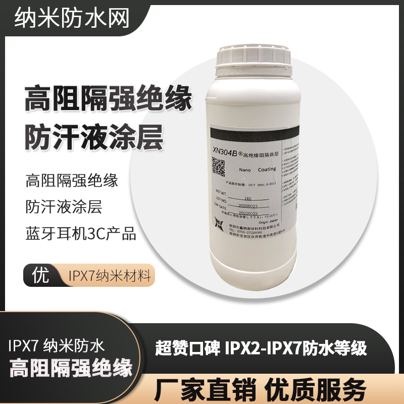
高阻隔强绝缘防汗液涂层蓝牙耳机3C电子产品IPX7纳米材料
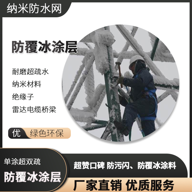
耐磨超疏水纳米材料 绝缘子架空导线电缆桥梁防覆冰涂层
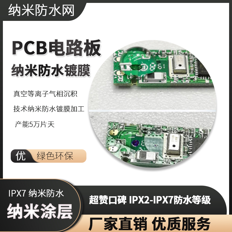
真空等离子气相沉积技术纳米防水镀膜加工 产能5万片天
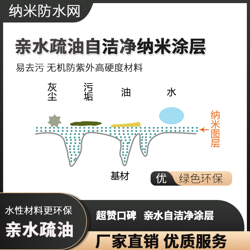
亲水疏油自洁净纳米涂层 易去污 无机防紫外高硬度材料
台湾超亲水防雾塑料专用 附着力好 透过率高 持久有效